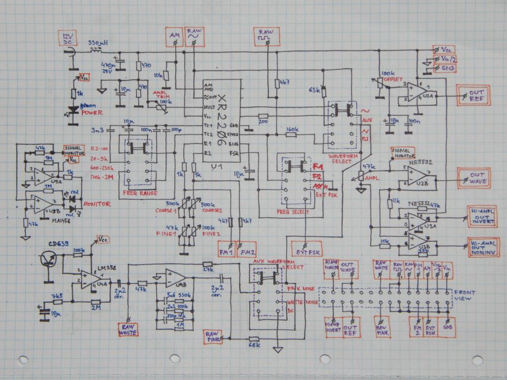
The XR2206 is a classical chip used in many low-cost low-grade frequency/function generators. It can provide fairly good sine and triangle wave output, square wave, and can be also tricked into asymmetric duty cycle.
The original inspiration was taken from here ,
and more functions were added.
,
and more functions were added.
The core of the design is the XR2206 chip. It is used in its datasheet circuit.
The chip has two inputs for frequency setting, selected between with the FSK input. This allows the chip to be used for frequency-shift keying. This also allows, according to the datasheet, to use the chip for ramp and PWM generation, when the FSK input (pin 9) is connected with the SYNCO output (pin 11) - this however does not work entirely well at higher frequencies, when certain combinations of resistances on the two inputs cause oscillations near the SYNCO signal edge.
There are two sets of pots for adjusting the frequency; a switch can select which one should be used - the first one, the second one, both (where the first set controls the duration of one half of the signal and the other one controls the other half, which is useful for ramp and PWM signals), or external select (where a FSK input on the connector is used).
The coarse frequency range is chosen by a switch using four different capacitors. The range setting is common for both the resistor inputs.
The chip's output amplitude differs wildly between the triangle and the sine, by about 3 times. The difference against the square wave output, achieved by a pullup on the open-collector SYNCO output, is even more significant.
The output amplitude is selected by a potentiometer. The relative amplitude of the different types of signals can be adjusted by connecting a resistor in series to the pot, attenuating them by a factor to make them roughly similar amplitude.
To isolate the generator from the output, an output buffer was used. A NE5532 chip was selected on the basis of availability and cost; the earlier-used LM358 was found to be inadequate at high frequencies, losing gain rapidly.
The output signal is relative to half of the power supply voltage. As signals with different offsets are often needed, an offset output is made from an op-amp buffer fed from a simple resistor divider potentiometer. This provides a DC signal with adjustable level.
For higher-amplitude needs, there is a differential amplifier stage. Another NE5532 chip is used as a pair of inverting-noninverting amplifiers, producing a symmetrical output. This allows virtually doubling the output voltage swing when the load is connected between the symmetrical outputs. The gain of the amplifier is set to allow as high as possible amplitude without significant clipping at the highest output level set.
For some needs, a noise instead of signal can be desired. A simple noise generator was built around a LM358 op-amp, using the emitter-base junction of a transistor in its reverse-breakdown mode. This is one of the classical approaches.
The circuit chosen to use was this one,
with a few changes. There are better generators out there, but this one won on the
basis of simplicity.
To allow its use as both white and pink noise generator, the gain of the first stage was increased and the gain of the second stage was lowered, so the output levels aren't clipped and can be directly fed into the output buffer and differential amp.
2.2 µF ceramic capacitors were chosen instead of 10 µF nonpolarized electrolytics on the basis of size and availability. A different transistor was chosen as the noise source on the basis of availability and selected for the highest noise from several candidates. The capacitors for the pink noise filter were assembled from multiple ones due to lack of immediate availability of the desired values.
It was found that a visual indication of the output signal is beneficial in many cases. A simple circuit similar to the differential amplifier in the output buffer stage was used. An old MA1458 op-amp was chosen on the basis of availability and desire to dispose of the ancient chips with lousy parameters. The gain of the inverting and noninverting stages was chosen to be more or less the same, and the output indication was done by a pair of antiparallel red LEDs.
At low frequencies the output levels can be seen as the LEDs flashing. At higher frequencies the brightness of the LEDs shows the output level and their relative brightness shows the duty cycle in case of asymmetric waveform selection.
The circuit works well up to above 100 kHz, where it gradually loses gain and symmetry and then ceases to function entirely. This can be alleviated by using a different op-amp, e.g. the NE5532, if it ever becomes annoying enough.
It was found that some switching power supplies have pulses on their output. (Well, duh.) And that these pulses tend to propagate to the output of the signal generator. (Oops.) A 330 µH choke was chosen on the basis of availability and successfully tested as a power filter.
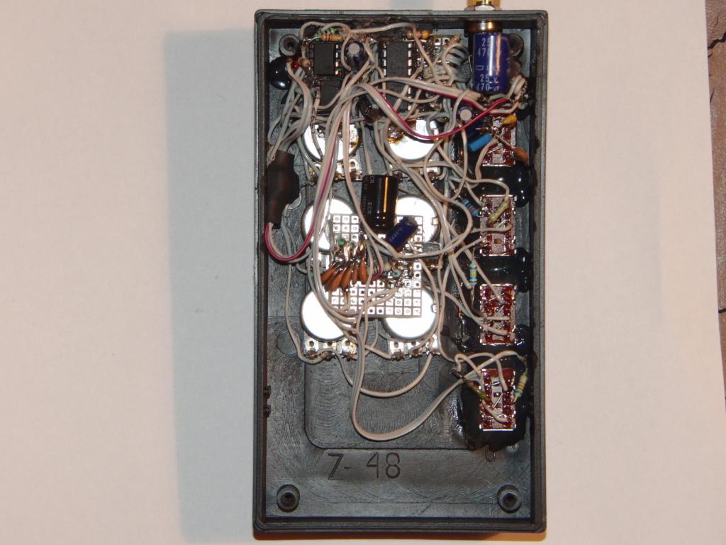 Inside view | 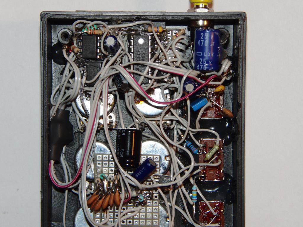 Electronics detail | 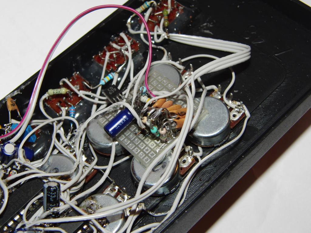 Noise generator module | 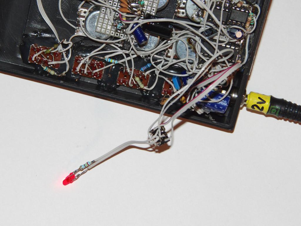 Monitor circuit |
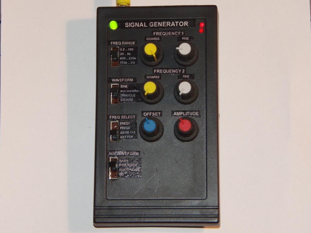 Case, front | 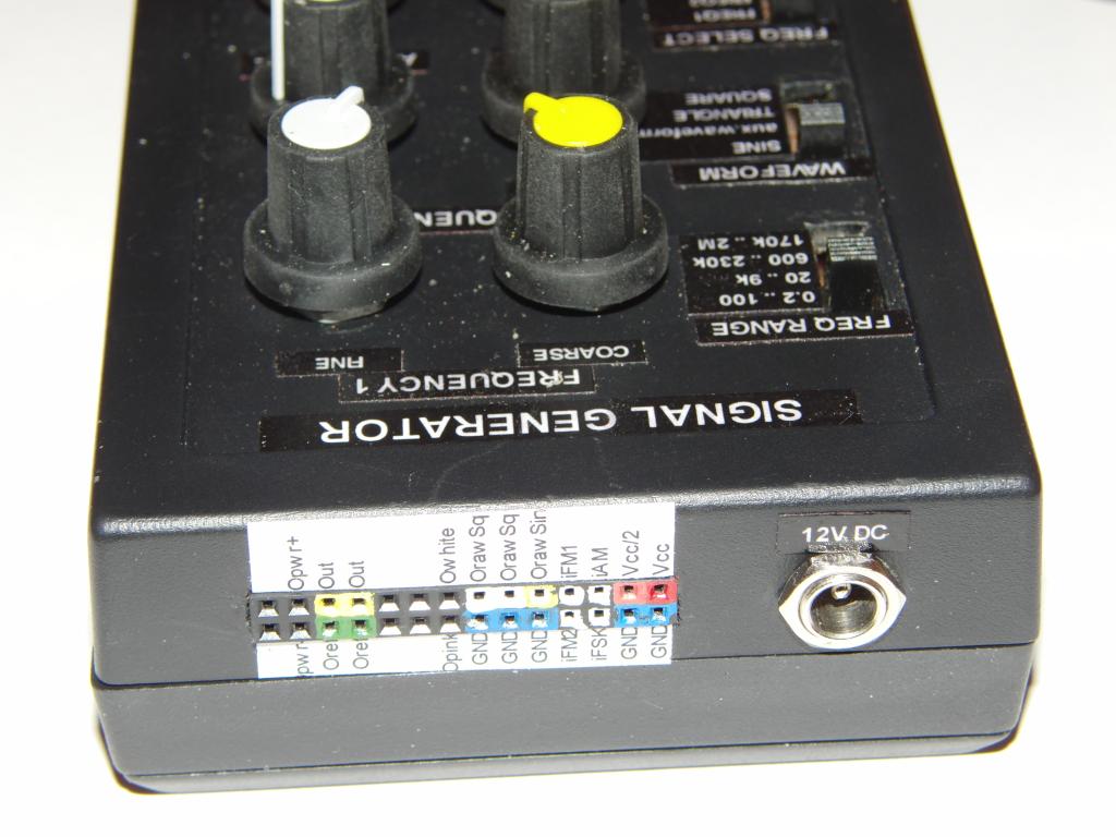 Outputs |